


What is a Diode?
A diode is a device which only allows
unidirectional flow of current if operated within a rated specified voltage
level. A diode only blocks current in the reverse direction while the
reverse voltage is within a limited range otherwise reverse barrier breaks and
the voltage at which this breakdown occurs is called reverse breakdown voltage.
The diode acts as a valve in the electronic and electrical
circuit. A P-N junction is the simplest form of the diode which behaves as
ideally short circuit when it is in forward biased and behaves as ideally open
circuit when it is in the reverse biased. Beside simple PN junction diodes,
there are different types of diodes although the fundamental
principles are more or less same. So a particular arrangement of diodes
can convert AC to pulsating DC, and hence, it is sometimes also called as a
rectifier. The name diode is derived from "di-ode" which means a
device having two electrodes.
Symbol of Diode
The symbol of a diode is shown below, the arrowhead points
in the direction of conventional current flow. We can create a simple PN
junction diode by doping donor impurity in one portion and acceptor
impurity in other portion of silicon or germanium crystal block. These make a p
n junction at the middle part of the block beside which one portion is p-type
(doped with trivalent or acceptor impurity), and another portion is n-type
(doped with pentavalent or donor impurity). It can also be formed by joining a
p-type (intrinsic semiconductor doped with a trivalent impurity) and n-type semiconductor
(intrinsic semiconductor doped with a pentavalent impurity) together with a
special fabrication technique such that a p-n junction is formed. Hence, it is
a device with two elements, the p-type forms anode and the n-type forms the
cathode. These terminals are brought out to make the external connections.
Working Principle of Diode
N - side will have a significant number of electrons, and
very few holes (due to thermal excitation) whereas the p side will have a high
concentration of holes and very few electrons. Due to this, a process called
diffusion takes place. In this process free electrons from n side will diffuse (spread)
into the p side and recombine with holes present there, leaving positive
immobile (not moveable) ions in n side and creating negative immobile ions in p
side of the diode. Hence, there will be uncovered positive donor ions in n -
type side near the junction edge. Similarly, there will be uncovered negative
acceptor ions in p - type side near the junction edge. Due to this, numbers of
positive ions and negative ions will accumulate on n - side and p - side
respectively. This region so formed is called as depletion region due to the
“depletion” of free carriers in the region. Due to the presence of these
positive and negative ions a static electric field called as "barrier
potential" is created across the p n junction of the diode. It is called
as "barrier potential" because it acts as a
barrier and opposes the further migration of holes and
electrons across the junction.
Forward Biased Diode
In a PN junction diode when the forward voltage is applied
i.e. positive terminal of a source is connected to the p-type side, and the
negative terminal of the source is connected to the n-type side, the diode is
said to be in forward biased condition. We know that there is a barrier
potential across the junction. This barrier potential is directed in the
opposite of the forward applied voltage. So a diode can only allow current to
flow in the forward direction when forward applied voltage is more than barrier
potential of the junction. This voltage is called forward biased voltage. For
silicon diode, it is 0.7 volts. For germanium diode, it is 0.3 volts. When
forward applied voltage is more than this forward biased voltage, there will be
forward current in the diode, and the diode will become short circuited. Hence,
there will be no more voltage drop across the diode beyond this forward biased
voltage, and forward current is only limited by the external
Forward Biasing Characteristic of Diode
When, P terminal is more positive as compared to N terminal
i.e. P- terminal connected to positive terminal of battery and N-terminal
connected to negative terminal of battery, it is said to be forward biased. Positive terminal
of the battery repels majority carriers, holes, in P-region and negative
terminal repels electrons in the N-region and push them towards the junction.
This result in increase in concentration of charge carriers near junction,
recombination takes place and width of depletion region decreases. As forward
bias voltage is raised depletion region continues to reduce in width, and more
and more carriers recombine. This results in exponential rise of current.
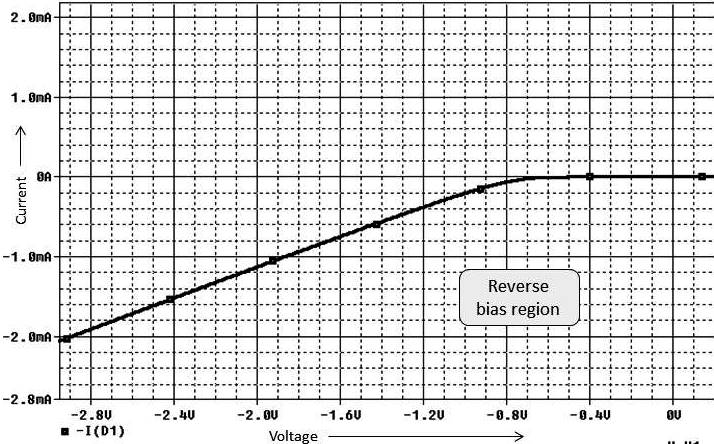
Reverse Biasing Characteristic of Diode
In reverse biasing P- terminal is connected to negative
terminal of the battery and N- terminal to positive terminal of battery. Thus
applied voltage makes N-side more positive than P-side. Negative terminal
of the battery attracts majority carriers, holes, in P-region and positive
terminal attracts electrons in the N-region and pull them away from the
junction. This result in decrease in concentration of charge carriers near
junction and width of depletion region increases. A small amount of current
flow due to minority carriers, called as reverse bias current or leakage
current. As reverse bias voltage is raised depletion region continues to
increase in width and no current flows. It can be concluded that diode acts
only when forward biased. Operation of diode can be summarized in form of I-V diode
characteristics graph. For reverse bias diode, V<0, ID =
IS Where, V = supply voltage ID = diode current IS
= reverse saturation current For forward bias, V > 0, ID = IS(eV/NVT
- 1)
Where, VT = volt’s equivalent of temperature = KT/Q = T/11600 Q =
electronic charge = 1.632 X 10 - 19 C K = Boltzmann’s constant =
1.38 X 10 - 23 N = 1, for Ge = 2, for Si As reverse bias voltage
is further raised, depletion region width increases and a point comes when
junction breaks down. This results in large flow of current. Breakdown is the
knee of diode characteristics curve. Junction breakdown takes
place due to two phenomena: How Diode Works?
Diode operates in forward bias or in reverse bias mode. Let’s consider ideal diode first. When ideal diode is forward biased, it will short circuit (turn ON)and conducts current. When diode is reverse biased, it will open circuit (turn OFF) and no current flows through it. The VI characteristics of ideal diode is linear and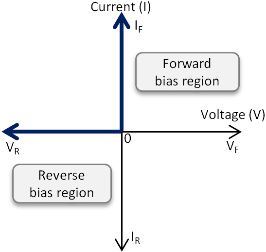
VI Characteristic of Ideal Diode
There is not much difference in ideal and practical diode characteristics. Practically some power is consumed by diode during forward bias. It will not block all reverse current when reverse biased. This power consumed during forward bias is defined in terms of forward voltage. This voltage is also known as cut-in or knee voltage. It is ~0.7V for Silicon and ~0.3V for Germanium. The practical forward voltage varies with current, temperature and type of diode used. Let’s see practical diode characteristics with following examples.
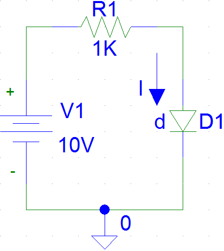
Example 1 – Diode in forward bias
Example of Forward Biased Diode
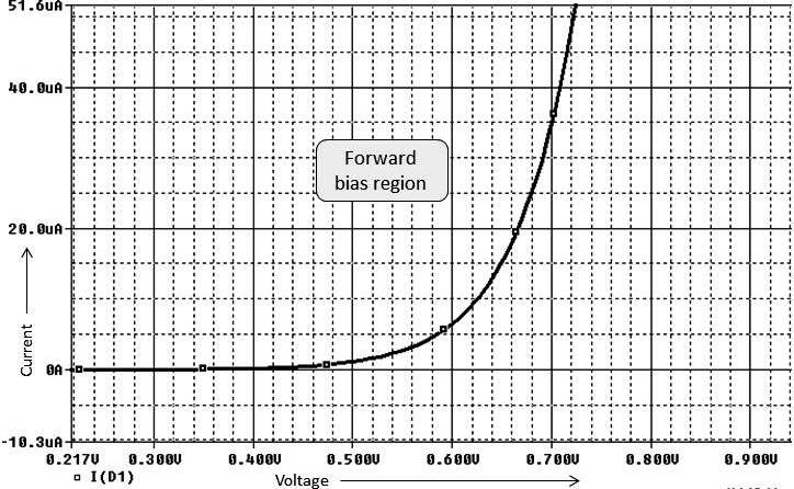
In forward bias, practical diode acts as a short circuit when input voltage is greater than forward voltage (VF ). During positive forward voltage, significant amount of current flows through diode called as forward current. The waveform below shows simulation of VI characteristics of forward biased diode. The current in forward bias is usually in miliamps. Here, resistor present between voltage source and diode minimizes current to microamps.
0 comments:
Post a Comment